Product
- Automatic-Reflow Line eries
- V-CUT & slop-edge equipment
- Drill and punch equipment
- Semiconductor packaging transfer molding press
- Automatic Machine
- FPCB&RPCB Exposing equipment
- FPCB&RPCB Visual inspection machine
- FPCB&RPCB Printing facilities
- FPCB&RPCB press machine
- FPCB&RPCB Wet process Surface Treatment Equipment
- Screen Film Loop inspection device
- process equipment for touch control products
- Developing device
- Welding Machine
- OTHER MACHINE
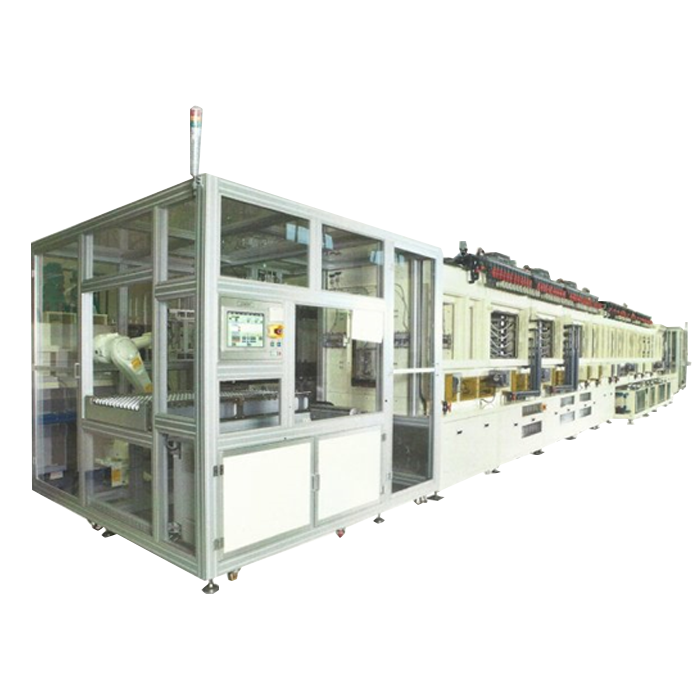
Non-contact developing M C
Scope:
Non-contact developing M C
Uses:
The device is suitable for high-resolution and high-productivity IC package circuit board, the device is non-contact imaging development, the substrate damage can be minimized to achieve high-resolution.
Features:
1. Thickness: Min 0.04,Max 0.5mm
2. Line space:15um
3. PCB substrate damage to minimize
- droop, scratches, graphic skew and short circuit.